Tagged with

Printed Electronics

Latest Posts

Sometimes manufacturers would like to install heating in objects that are difficult to heat. The armrest of your car. Your sporty winter coat. Bags for food delivery. Sleeping bags. etc This has been difficult to achieve until now. Read more about printed heater technology

The advantages and functioning of PTC heaters

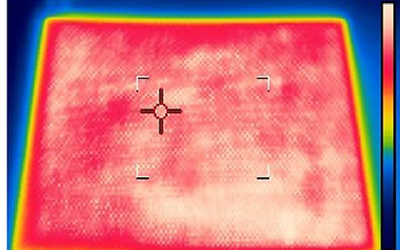
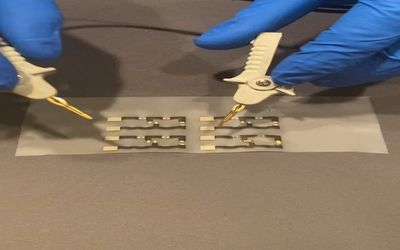
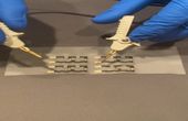
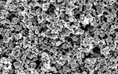
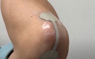
Wearable electronic textiles are a demanding environment for reliable interconnects – the ability to function with movement and survive multiple cleanings and reuse. Good adhesion is particularly challenging in these wearable and conformable electronics applications. While solders provide the most conductive electrical connection, they are rigid and require not only the addition of an underfill adhesive but usually a post bond encapsulation. This Anisotropic Conductive Epoxy, provides reliable interconnections between electronic components and circuitry on textiles with excellent structural bonding, without encapsulation, even under repeated stretching and washings. This technology has been shown as a scalable assembly process for e-Textile manufacturing in an SMT line.

Reliable, Scalable, Anisotropic Interconnect Solution for Wearable Electronics

The progress of screen printing towards fine line printing has been incredible going from 100 µm features before 2010 to 70 µm to 2015 to 40 µm in 2018 and now pushing - in development- towards 20 µm and less. In parallel, the wet thickness of the printed line have gone down from 12um or so in 2018 to now just 4um.

The three themes are closely linked since QDs can be digitally printed as color conversation materials atop blue microLEDs to enable wide color gamut RGB uLED displays without requiring a separate transfer step for each color.. This is an important technology as it simplifies the manufacturing step for microLED and thus removing a major hinderence.

PCB layers are the copper layers within a printed circuit board, laminated between or onto layers of conductive material. These layers are stacked to enhance the functionality of electronic devices. This article explores the concept of PCB layering, the various types of layers, and their benefits.

PCB Layers: Everything You Need to Know

As NASA prepares to send astronauts back to the Moon to live and explore, capabilities for space-based manufacturing of sensors, circuits, and other electronics will become increasingly critical. Recent microgravity flights have helped to advance cutting-edge methods for 3D printing of electronics

Microgravity Testing Advances Space-Based Printing of Electronics

Profiles