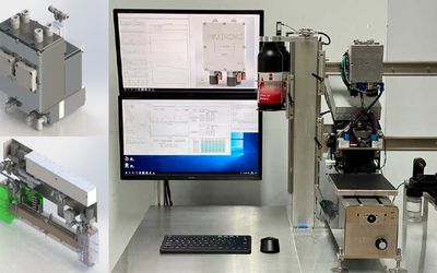
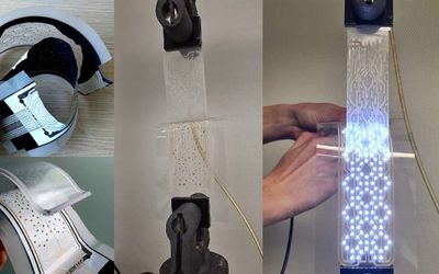
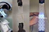
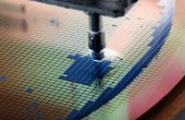
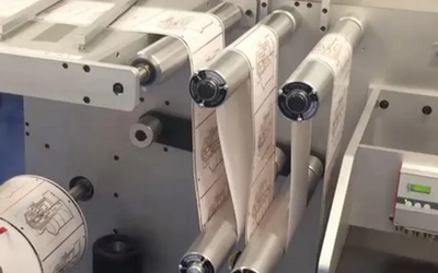
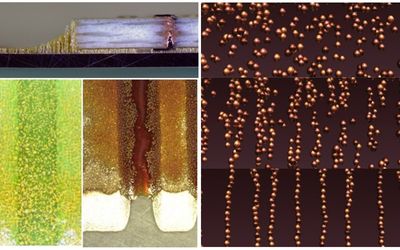
Tagged with

Printed Electronics

Latest Posts

Silicon has emerged as the most widely used semiconductor material in the electronic industry, paving the way for the digital age. However, many are still oblivious to the unique properties and characteristics that make silicon ideal for a range of applications. This article explores the fundamentals of semiconductor materials, the properties of silicon that make it a prominent player in the semiconductor industry, and its diverse applications in electronic devices.

Silicon Semiconductor: A Comprehensive Guide to Silicon and its Use in Semiconductor Technology

The key enabler for reliable device fabrication in printed electronics is functional inks with tunable electrical properties incl. conductivity, dielectric strength & electrical resistance. Here, you will learn about unique polyimide based pastes able to withstand temperatures up to 300°C.

Innovative High-Temperature Inks for Printed Electronics

Castellation PCB is a type of printed circuit board (PCB) that has a series of small, plated through holes along the edges of the board. These holes are used to create a connection between the board and other components in a circuit. This article delves into the design, manufacturing, and testing processes involved in creating castellation PCBs, providing insights into the key considerations and guidelines that engineers and manufacturers should follow to optimize their designs for performance, reliability, and manufacturability.

Castellation PCB: A Comprehensive Guide to Design, Manufacturing, and Applications

Status and evolution of intelligent skin patches, enabled by flexible hybrid electronics, going from a single wired sensors to complex wireless multi-function capability. Learn about trends, archirectures and challenges from a manufacturer's point of view to understand how to design for production.

Smart Skin Patches and Noninvasive Medical Sensing

Semiconductors are the building blocks of modern electronics, powering everything from smartphones to satellites. This in-depth guide provides a comprehensive understanding of semiconductors' engineering principles and applications, delving into their fundamental concepts, materials, devices, manufacturing processes, and their impact on today's technology landscape.

What is a Semiconductor? A Comprehensive Guide to Engineering Principles and Applications

Wafer backgrinding is a crucial step in semiconductor manufacturing, as it prepares the wafer for further processing and packaging. The procedure comprises the thinning of silicon wafers by scraping out material from the backside, which is crucial for enhancing the functionality and dependability of semiconductor devices. This article examines the wafer backgrinding procedure, its difficulties, and the significance of quality control in ensuring the production of high-quality semiconductor devices.

Wafer Backgrinding: An In-Depth Guide to Semiconductor Manufacturing

In wearables, the design on paper often does not work in practice. In this world, your idea may only go as far as your chosen contract manufacturer can take you. It is the key role of the contract manufacturers to help you make the vital adjustment to make your product a success.

How far can we flex?

Profiles