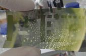
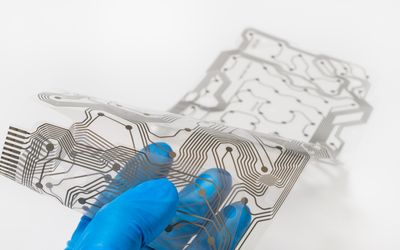
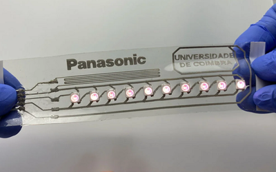
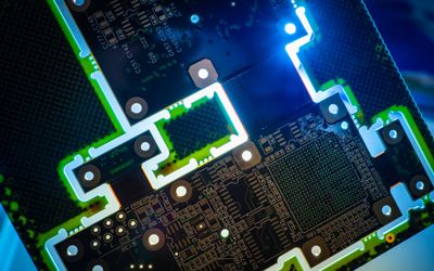
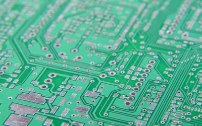
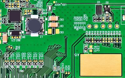
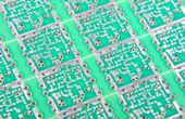
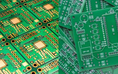
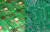
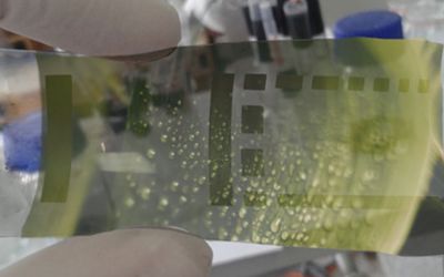
Tagged with
Printed Electronics
Latest Posts
Die attach, also known as die bonding or die mount, is a process used in the semiconductor industry to attach a silicon chip to the die pad of a semiconductor package's support structure, such as a leadframe or metal can header. This article explores the fundamentals of die attach, its importance, materials, and methods used in die attach, its parameters, quality, and reliability techniques.
Review of industrial applications of printed electronics - what are current successful applications?
TechBlick's presentation reviews printed electronics' industrial applications, dispelling the notion that it's solely a technology of the future. The talk showcases various commercial success stories incl. photovoltaics, displays, sensors, HMIs, 3D electronics, MLCCs, PCBs, semicon packaging, etc
Filled vias are via holes that are completely filled and closed with conductive or non-conductive material or copper plating. The filled via is one of the many realizations of PCB via covering, specified by industry standards. This article covers the definition, benefits, processes, applications, and challenges of filled vias.
PCB Panelization is a PCB manufacturing technique. It involves the grouping of several small printed circuit boards to form a single array, which is known as a panel. Panelization is commonly employed in PCB manufacturing because it saves time and cost. This article discusses the conditions, design considerations, methods, types, and benefits of PCB panelization.