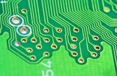
The silkscreen is a layer on the surface of a PCB that is used to identify a lot of information about the electronic printed circuit board.
Tagged with
semiconductors
Latest Posts
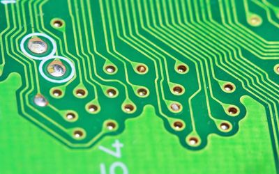
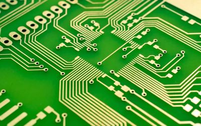
Vias are small holes in a PCB that enable electrical connections between different layers of the board. In the context of PCB design, via tenting refers to the process of covering the vias with a protective layer, typically a solder mask or dry film. This protective layer shields the vias from environmental factors, such as dust, moisture, and chemicals, which can lead to corrosion or short circuits. As PCB technology continues to advance, the importance of via tenting in maintaining the performance and reliability of complex, high-density interconnect (HDI) and flexible PCB designs cannot be overstated. This guide explores the art and science of via tenting, shedding light on its significance, techniques, and applications in modern PCB design and manufacturing.

As an Inspiring 50 award-winner and startup founder, Greek-Albanian Sophia-Eriola Shanko is a first-time entrepreneur. She has a BSc in Control Systems Engineering, graduating in a classroom with two girls and 100 boys. She pursued a fully EU-funded MSc on Semiconductors and obtained her Ph.D. at TU Eindhoven.

5 minutes read

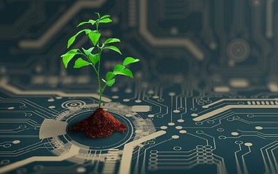
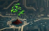
‘Smart Circularity’—the circular economy as it relates to connected technology and the IoT—can help the world shift away from linear consumption to an economy where resources are fed back into a closed loop of recycling, reusing and sharing.

4 minutes read
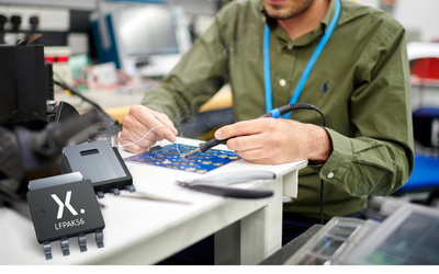
More than 20 years ago, a team set out to solve a problem: How do we reduce power loss and help reduce MOSFET size at the same time? LFPAK was the answer - and it changed everything.
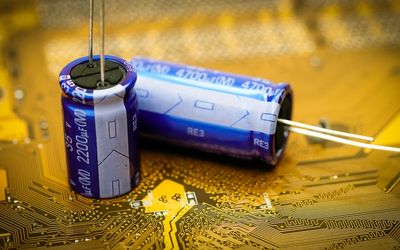
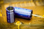
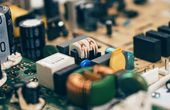
Capacitors store electrical energy, similar to batteries, and are used in many electronic devices. Due to their voltage-storing nature, handling them can be dangerous. This article outlines various techniques and safety measures to safely discharge capacitors.
Manufacturing platform, Hubs, has published its Supply Chain Resilience Report 2023, featuring insights from 2022 and addressing recent supply chain disruptions, including the ongoing war in Ukraine, escalating tensions between China and Taiwan, and more. Download the full report below.

This article delves into the various aspects of cleaning circuit boards, from understanding the basics and identifying the need for cleaning to the actual cleaning process, maintenance, and when to seek professional help.
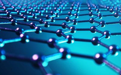
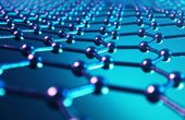
For the first time, ETH Zurich researchers have been able to make a superconducting component from graphene that is quantum coherent and sensitive to magnetic fields. This step opens up interesting prospects for fundamental research.

3 minutes read
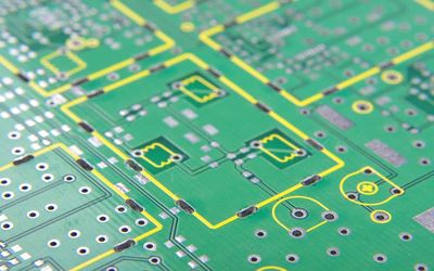
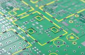
PCB traces are fundamental components in circuit design, serving as the pathways for electrical signals. This article examines the advancements, applications, and challenges of PCB trace technology. Discover insights into optimizing designs and overcoming common obstacles in PCB trace implementation.
This article delves into the core variations between PMOS and NMOS, exploring their fundamentals, structural differences, operating principles, and practical applications.

Article #4 of the "Why Edge?" Series. A short guide to how Edge AI is enabling cutting-edge advances in the automotive industry.


Article #4 of the Enabling IoT Series. Industrial enterprises are moving to a new approach to asset management, namely predictive maintenance by leveraging powerful new sensors and data.

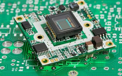
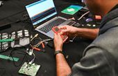
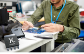
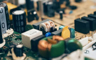
Circuit card assemblies (CCA) give birth to a complete printed circuit board (PCB) after assembling every component. A printed circuit board has no electrical components and needs to go through a manufacturing process called circuit card assemblies which are the complete board assembly.
Article #5 Electronics Innovation Series. IoT security is a shared responsibility between chip manufacturers, hardware designers, and the consumer.