Article #2 of the "Why Edge?" Series. Edge AI increases battery life, reduces latency, and in many cases, eliminates the need for cloud communication, making wearable devices more user-friendly and secure.
Tagged with
semiconductors
Latest Posts


For the length of human history, technology has played an important role in preventing theft. Before car keys, Henry Ford had to chain his car to a lamppost to avoid anyone with the strength to turn a physical crank from stealing it.

4 minutes read


The challenges of EV charging must be addressed quickly to ensure the rapid adoption of electric transportation.

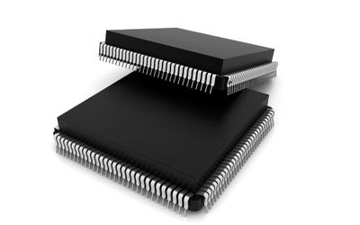
Integrated circuit (IC) package types encompass a range of protective enclosures designed to shield semiconductor components from physical damage and corrosion. This article explores the various classifications of IC packages, each tailored to specific requirements and applications.
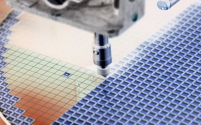
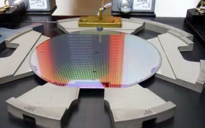
Chips and wafers are the integral components of a semiconductor device. Find out the differences between chip wafers and chips and understand their role in semiconductor manufacturing.
A short guide to understanding the edge neural network design.


Proven benchmarks provide a structured method for comparing ML/DL products and services.

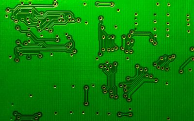
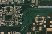
Printed Circuit Board Vertical Interconnect Access (PCB VIAs) are small plated holes that create electrical connections between different circuit board layers. This article delves into the various types, functions, and best practices of PCB VIAs to help you optimize your PCB design.

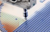
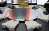
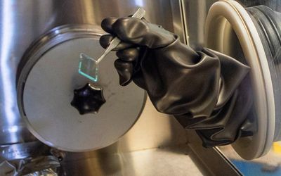
Wafer thinning is a part of the semiconductor manufacturing process. It is essentially grinding off the backside of the wafers to control their thickness and is useful for the production of ultra-thin wafers. These flattened wafers are used to effect stacked and high-density packaging in compact or microelectronic devices. This article discusses the meaning of wafer thinning, along with its various techniques and significance.
Conformal EMI shielding is a megatrend on its way to become ubiquitous in electronics. The incumbent process is based on sputtering a tri-layer structure consisting of SUS on the EMC of the package. In these slides, you can see performance analysis and detailed cost analysis/projections.

2 minutes read
The new approach moves energy efficiently and could reduce energy losses converting light into electricity.

3 minutes read

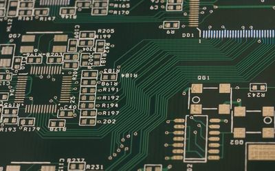
PCB layers are the copper layers within a printed circuit board, laminated between or onto layers of conductive material. These layers are stacked to enhance the functionality of electronic devices. This article explores the concept of PCB layering, the various types of layers, and their benefits.
Article #4 Electronics Innovation Series. Alternative SBC’s and customer-orientated manufacturing will ease supply chain conditions.

5 minutes read

Article #3 of the Enabling IoT Series. This article looks at how Time of Flight (ToF) sensors are used for this purpose and are changing the way we can interact with VR, and other video technologies.

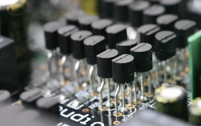
This article delves into the specifics of NPN and PNP transistors, their working principles, applications, comparisons, and factors to consider when choosing between them.