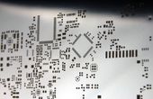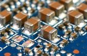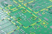
Before sending your final design files to your CM for manufacturing, check out these useful tips and final steps.

4 minutes read
Tagged with
Before sending your final design files to your CM for manufacturing, check out these useful tips and final steps.
4 minutes read
In this article, we will go over everything you need to know about PCB stencils.
This article aims to provide a comparative analysis of HASL vs ENIG, providing valuable insights to aid in making informed decisions for PCB design and manufacturing.
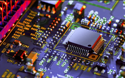
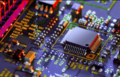
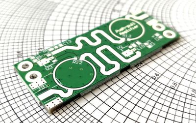
Engineers face persistent challenges with PCBA designs as they become more complex, posing a risk to the development process as a whole. Those who neglect design complexity may fall behind development schedules, incur expenses, and miss market deadlines.
6 minutes read
Approximately 7% of the world's gold can be found inside discarded electronic devices, in form of PCB Gold Fingers. While a tonne of Gold Ore produces just 5 grams of pure gold on average, a tonne of electronic scrap can house 300 grams of gold inside it. Here we gloss over the significance of gold fingers in the present day electronics industry and all kinds of gold fingers specifications you need to know.
This in-depth guide will delve into the fundamentals of I2C and SPI communication protocols, including their working principles, comparative advantages, system configurations, and practical applications in embedded systems and IoT devices.
Electrical engineers must continually seek out new options and keep up with market changes. Take note of these six trends within the electronics industry.
5 minutes read
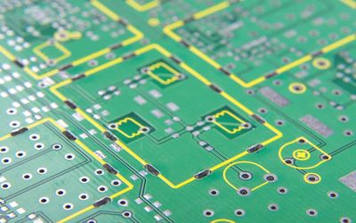
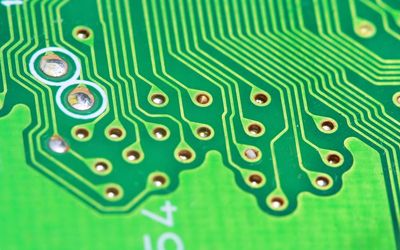
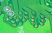
Vias go through two or more layers of PCBs to form an electrical connection. Making them right under the component’s pad saves space, reduces track inductance and simplifies design.
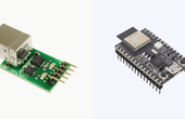
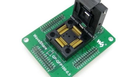
The right programming method will be determined by the volume of your assembly run and the form factor of your device.
3 minutes read
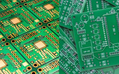
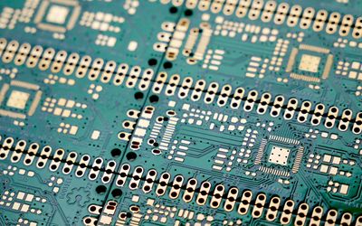
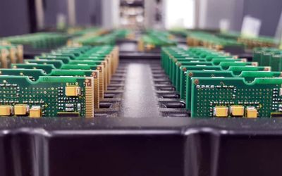
Printed Circuit Boards (PCBs) provide the foundation for the assembly of electronic components and enable the functionality of a wide range of devices. This article journeys through the requisite steps in the PCB manufacturing process, detailing the procedures involved in each.
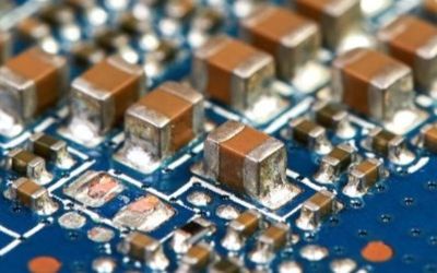
It's difficult to protect every signal from noise intrusions, but this must be done to design an effective PCB assembly.
3 minutes read
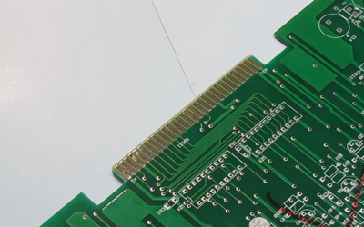
The silkscreen is a layer on the surface of a PCB that is used to identify a lot of information about the electronic printed circuit board.
PCBA design capabilities are crucial to the future of wearable technology. Wearables and PCBA design are inextricably linked since both have a significant influence on each other. As wearable devices become more popular, electronics designers and manufacturers are designing smaller, denser, and more flexible devices.
10 minutes read
Vias are small holes in a PCB that enable electrical connections between different layers of the board. In the context of PCB design, via tenting refers to the process of covering the vias with a protective layer, typically a solder mask or dry film. This protective layer shields the vias from environmental factors, such as dust, moisture, and chemicals, which can lead to corrosion or short circuits. As PCB technology continues to advance, the importance of via tenting in maintaining the performance and reliability of complex, high-density interconnect (HDI) and flexible PCB designs cannot be overstated. This guide explores the art and science of via tenting, shedding light on its significance, techniques, and applications in modern PCB design and manufacturing.
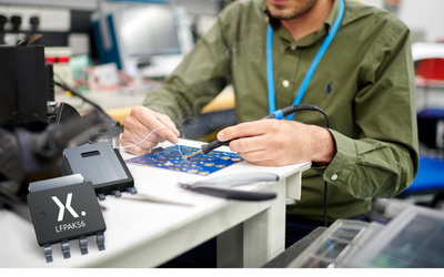
More than 20 years ago, a team set out to solve a problem: How do we reduce power loss and help reduce MOSFET size at the same time? LFPAK was the answer - and it changed everything.