NANOWEB® is an extremely thin, transparent, conductive film that consists of an invisible, nanostructured metal mesh fabricated onto a glass or plastic surface. With its unrivaled transparency, conductivity, and flexibility, this patented functional film holds immense potential for both passive and powered use cases, with applications including electromagnetic interference shielding, antennas, 5G/6G redirection systems for elimination of dead spots, and deicing/defogging devices for vehicle windows and eyewear.
Tagged with
electronics
Latest Posts

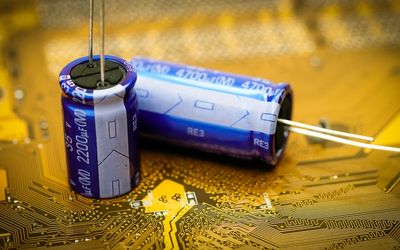
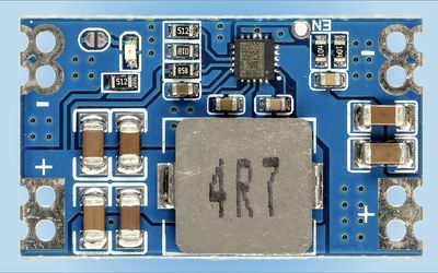
Capacitors store electrical energy, similar to batteries, and are used in many electronic devices. Due to their voltage-storing nature, handling them can be dangerous. This article outlines various techniques and safety measures to safely discharge capacitors.


What to know about the benefits of domestic prototyping

4 minutes read


Find out what this complex piece of legislation means for electronics manufacturing.

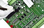
This article delves into the various aspects of cleaning circuit boards, from understanding the basics and identifying the need for cleaning to the actual cleaning process, maintenance, and when to seek professional help.

Article #5 of the Enabling IoT Series. MEMS microphones can deliver high-quality sound in an ultra-small form-factor.

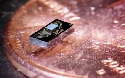
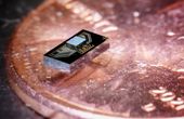
Engineers at Caltech and the University of Southampton have collaboratively designed an electronics chip integrated with a photonics chip (which uses light to transfer data)—creating a cohesive final product capable of transmitting information at ultrahigh speed while generating minimal heat.

3 minutes read
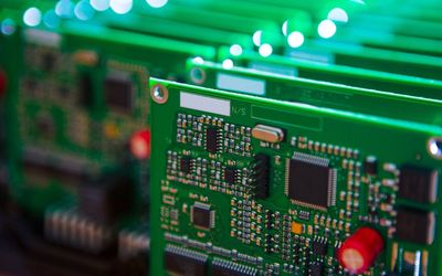
PCBs are extensively used across industries, powering devices from simple gadgets to complex systems. In this article, we’ll understand the importance of PCB thickness, the various factors affecting it, and its impact on design and other factors.

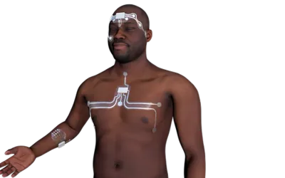
In this episode, we talk about the tattoo-like flexible wearable technology that’ll provide seamless high precision health monitoring for patients and enthusiasts.


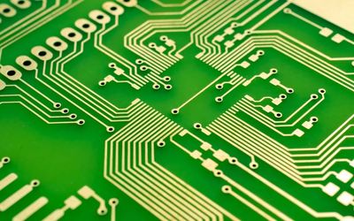
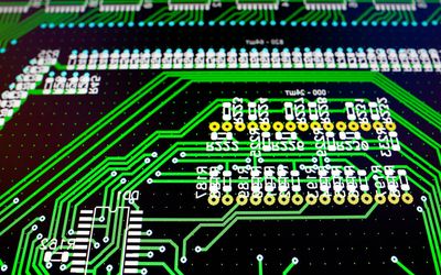
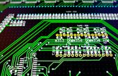
PCB traces are fundamental components in circuit design, serving as the pathways for electrical signals. This article examines the advancements, applications, and challenges of PCB trace technology. Discover insights into optimizing designs and overcoming common obstacles in PCB trace implementation.
With some foresight, most CAD design layout packages can accommodate castellated edge designs.
3 minutes read
Bringing a product to market late has a real and negative impact on profits and brand reputation. In this blog, we go through the types of documentation your project requires and ways to streamline processes.
3 minutes read

This article delves into the core variations between PMOS and NMOS, exploring their fundamentals, structural differences, operating principles, and practical applications.


Article #6 of Power Management for Tomorrow’s Innovations Series: Power supplies for vehicle asset-tracking devices must be designed to operate at different voltage-current levels, be compact, and offer protection during transients and electrical faults.


Article #4 of Power Management for Tomorrow’s Innovations Series: This article investigates the effect that power designs have on the phase noise of Radio Frequency amplifiers through an experiment comparing the performance of three power regulators at different frequencies.