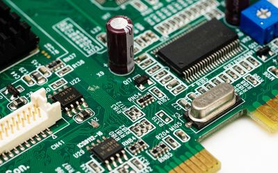
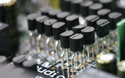
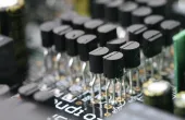
This article delves into the various types of SMD components, detailing their sizes, functions, soldering techniques, selection guidelines, and applications.
Tagged with
microchips
Latest Posts
This article provides a detailed guide to System in Package technology, its advantages and challenges, key components, design, and manufacturing process.
This article provides a detailed overview of the solder reflow process, types of reflow ovens, temperature profiles, solder paste composition and selection, reflow process potential challenges, solutions, inspection, and quality control techniques.
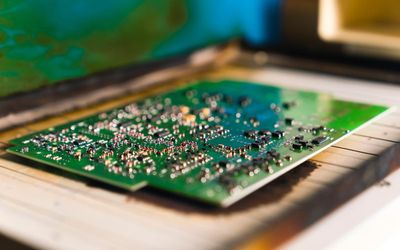
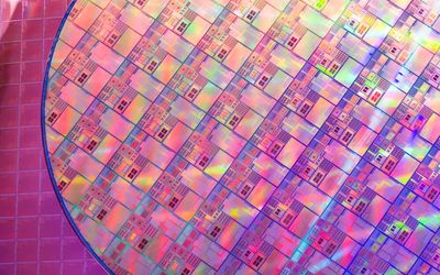
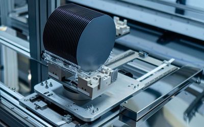
Wafer dicing separates individual integrated circuits or chips from a semiconductor wafer without damaging their delicate structures and circuits. This process is crucial for the production of electronic devices and components used in various industries, and the demand for it has increased with the development of high-performance and smaller electronic devices. Different dicing techniques, such as blade dicing, laser dicing, and plasma dicing, have been developed, and new innovations continue to emerge to address the challenges of complex semiconductor devices.
Many companies are now looking at alternatives to silicon chips.

5 minutes read
Electrical engineers must continually seek out new options and keep up with market changes. Take note of these six trends within the electronics industry.
5 minutes read
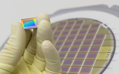
Chips and wafers are the integral components of a semiconductor device. Find out the differences between chip wafers and chips and understand their role in semiconductor manufacturing.
This article delves into the specifics of NPN and PNP transistors, their working principles, applications, comparisons, and factors to consider when choosing between them.
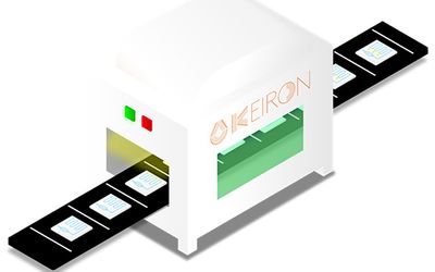
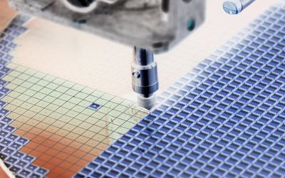
Meet Keiron Printing Technologies: the startup building the next generation microfabrication machine
A young team with a new technology are currently creating a revolution in the world of printed electronics. In their modern, brand-new lab at the High Tech Plaza, they will be developing a device that can deposit any material on any substrate at a very rapid pace.

6 minutes read


Axelera has recently joined the AI Innovation Center at High Tech Campus Eindhoven. The company is designing chips for AI on the edge with the aim to revolutionise the field and make AI accessible to everyone. They picked up an impressive 10 million euros in their seed investment round.
5 minutes read

Georgia Tech expert predicts that America will need to make major changes to the manufacturing and supply chain

3 minutes read

The semiconductor manufacturing field employs a range of etching techniques to craft intricate patterns and structures on material surfaces, with dry etching and wet etching being primary methods.
Silicon wafers are thin slices of highly pure crystalline Silicon, used in the production of integrated circuits. This article delves into the fascinating world of silicon wafers, unraveling their production process, unique properties, and the wide range of applications that make them indispensable.

This article provides a comparison between NB-IoT and LTE-M protocols and explores how NB-IoT facilitates energy-efficient and latency-tolerant IoT solutions for hard-to-reach locations.

10 minutes read


Reducing charge time is one of the remaining hurdles for EVs to overtake traditional cars in global sales. Combining digital control and silicon carbide (SiC) delivers level 3 or DC fast charging to reduce these charge times dramatically.

6 minutes read